Modern computing platforms are made of multiple hardware components, each with its own registers containing critical bits that carry nuanced meaning. Everything needs to be set just right in order to fully configure protection. As a result, there is little question why there are so many reports of vulnerabilities tied to missing protections across many systems from many vendors. Some examples include CVE-2014-8273 (Speed Racer), Skylake based MSI, Gigabyte BRIX BIOS Write Protection is not enabled (CLVA-2017-01-002), Coreboot, UEFI BIOS firmware analysis at scale, CVE-2018-4251, and slack Razer Laptop firmware controls.
How do these protections really work, though? Below, we will cover one mechanism for protecting firmware storage (e.g., SPI flash) from modification by malware in a bit more detail. While there are many more mechanisms to understand, vulnerabilities tied to this mechanism have taken on new importance with the discovery of Lojax malware that exploits this issue in the wild.
BOOT FIRMWARE
When your system starts, many things happen prior to the execution of the first instruction. When the processor starts execution, it does so at a specified location known as the reset vector. In order to boot properly, firmware needs to exist at the reset vector and properly configure the system such that the boot process can continue. (UEFI is a standard that defines one approach to this process.) For this discussion, we will look at how an attacker could modify the code executed in this boot process to undermine software-based security mechanisms.
The firmware mapped into the reset vector usually comes from an SPI flash chip on the motherboard. This is accessed through the SPI controller that is part of the chipset. Preventing access from software (including malware that gains control for whatever reason) is largely a matter of SPI controller configuration. Some configuration information can be stored on the SPI flash itself, inside the descriptor region. This defines access capabilities for each device that has access to the SPI flash through the controller. Additional configuration is accomplished by accessing registers documented in the chipset datasheet.
Many configuration registers support the concept of locking, which prevents reconfiguration after the lock is set. The configuration can only be changed again after a reboot. Similarly, the BIOS Control Register includes such a bit, known as BIOS Lock Enable (BLE). However, the actual behavior of this bit is not just to prevent further changes to the register until reboot. The datasheet for a recent chipset describes BLE in this way:

FIRMWARE STORAGE VULNERABILITIES
The function of BLE is to generate a special interrupt, called a System Management Interrupt (SMI), whenever writes to SPI are enabled. Code executing in System Management Mode (SMM) has the opportunity to decide what changes are allowed to system firmware, making it even more privileged than the OS kernel. The first security issue, then, is whether BLE is set at all, which comes up, for example, in this Skylake-based MSI system. In this case, the BIOS Write Enable (BIOSWE) bit can be set, and write operations to change firmware on SPI flash will work.
Why allow firmware to change at runtime? While it often makes sense to think about firmware as a small bit of code that configures the hardware and then transfers control away, this is not really how most systems work. Features such as modifying persistent data (storing firmware configuration or UEFI variables, for example) require the ability to write to SPI flash. Similarly, features that allow runtime update of firmware also require such access. If the hardware allows either of these things to happen at runtime, there must be some way to enable it.
To implement modification of SPI, software needs to enable writes (using BIOSWE), which generates a System Management Interrupt (SMI) to process the access control decision. If not authorized, the SMM code disables writes again and returns control to the normal runtime environment.
Did you spot the Race Condition? There is a time between enabling and disabling writes during which SPI commands can be independently processing write opcodes. Attackers can attempt write operations repeatedly in one thread while enabling flash writes (BIOSWE) in another. Many operations may be blocked, but eventually one will get through, and the process can be repeated until all writes are complete. This is known as the “Speed Racer” vulnerability (CVE-2014-8273), and it was described well by Corey Kallenberg and Rafal Wojtczuk in their Speed Racer paper back in 2015. Last year the vulnerability was exploited in the wild by Lojax malware.
To address this, we can require that the system actually be in SMM in order to allow SPI flash writes. This functionality is enabled by another bit in the BIOS Control Register called SMM BIOS Write Protection (SMM_BWP, or EISS in newer chipsets). When set, writes can only be allowed by code executing in SMM. This prevents the “Speed Racer” attack by bringing all threads into SMM, where trusted code can enable writes. When systems fail to set this configuration, as in CVE-2018-9069, they are vulnerable to the race condition attack.
These protections only control writes to the region of SPI flash containing system firmware for the host processor (known as the BIOS Region). To protect other regions (or as defense in depth for system firmware), it is also possible to program Protected Range Registers (PR0-PR4) in the SPI controller. Each of these registers defines a range of addresses and read/write access control permissions for the range. After setting these registers to control up to 5 regions, the configuration should be locked using the FLOCKDN bit so that it cannot be modified by software until a reboot. Of course, many systems fail to do this, as detailed by other researchers.
Chromebooks use a different mechanism to control writes to regions of the SPI flash. These systems use Coreboot instead of UEFI firmware. Coreboot is structured to separate a ROM stage from a RAM stage, and the earliest portion of firmware is protected with a physical screw that connects the write protect pin on the flash chip. That means changes to this early (trusted) firmware require physical access. While this limits what is available for software updates, it also puts a major barrier in place for malware to bypass protection of the root of trust for the system.
DETECTION
You can check these issues in a test lab using the open source CHIPSEC framework for platform security assessment. Specifically, these issues correspond to the bios_wp and spi_lock modules.


CHIPSEC results for firmware storage protections
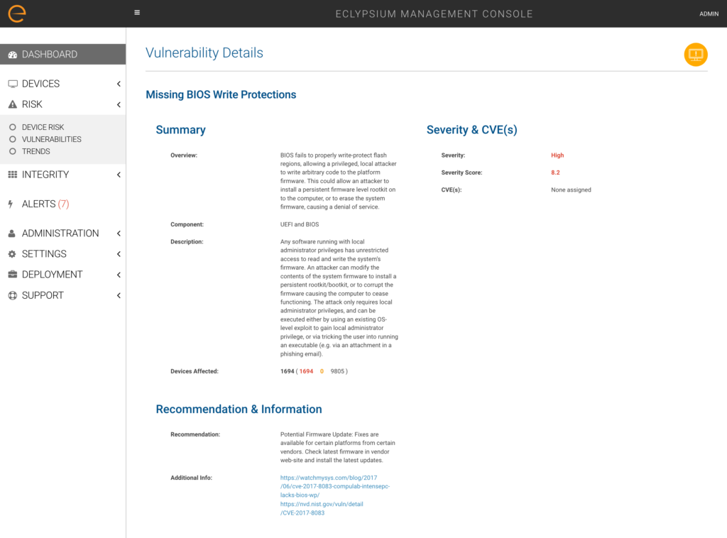
Eclypsium takes this into production systems in the enterprise, allowing you to vet systems when you first receive them—as well as continuously during operations. Our enterprise firmware protection platform scans laptops, servers and network devices for missing firmware storage protections—such as missing BIOS write protections that would enable a privileged attacker to bypass security. We also provide visibility into hardware misconfigurations, firmware that is out-of date or vulnerable to threats, and will detect and alert you to hardware implants, backdoors and rootkits.
Manufacturers often release firmware updates to address issues like these. When that happens, we help organizations identify which systems are vulnerable and locate updates to protect enterprise devices. There are many more aspects to defending the firmware and hardware attack surface across the variety of enterprise systems in use today. We will examine more in future posts.