
In this third (and final) post in the Firmware Security Realizations series (see Part 1 on Secure Boot and Part 2 on Intel ME) I will discuss one of the more common vulnerabilities I’ve discovered on several of my systems. In general, I’ve found missing BIOS write protections, the mechanisms implemented in firmware/hardware to protect writing to the SPI flash that contains firmware and configuration critical to allowing your computer to boot and function. Notice I used the term “protections” (plural) as I dug in and discovered there are quite a few ways in which protections can be implemented. BIOS write protections are somewhat complex which often leads to hardware manufacturers mixing up which bits should be set in order to get it right. The danger is that an attacker at the operating system level could modify your system at levels below Ring 0 to implant malware or even damage your system “permanently” (and is often difficult to remove).
As I was uncovering BIOS write protection vulnerabilities on select systems it became apparent that we have the same supply chain problems hinted at in the previous articles in the series. For Secure Boot, Intel ME/CSME, and BIOS write protections there is a combination of responsible parties that all have to “get things right” in order to deliver you a system with the best security configuration and then maintain that configuration. With BIOS write protections as an example, with some rare exceptions such as developer boards, you will want to rely on your hardware manufacturer for updates. The unique set of hardware and firmware that makes up your computer is a collection from multiple suppliers, and typically the hardware manufacturer is the main point in that supply chain defining what software and configuration will actually work (and not “brick” your system). We will cover many settings relating to your system hardware and firmware, please note we do not recommend changing these settings, and if you do, do so at your own risk.
Understanding SPI (As it relates to your BIOS)
In order to understand how write operations are governed on most computer systems today we need to dig into the SPI controller and the SPI flash. The SPI controller can be thought of as the access gateway to the SPI flash storage. You may wonder, as I did, why a system should even allow runtime changes to such critical firmware. The answer is basically for convenience. Remember when your computer had a floppy drive (I do, and yes I am dating myself now)? Before UEFI and modern BIOS architecture we used to update the BIOS by booting on physical media, such as a floppy disk. With the introduction of more complex hardware and firmware on modern computers we need a more convenient way to change settings and update firmware at runtime (e.g. to update Secure Boot variables as described in Part 1 of this series).
Let’s start with the layout of the SPI flash chip, which can differ from system to system but for the sake of this post can be depicted as follows:
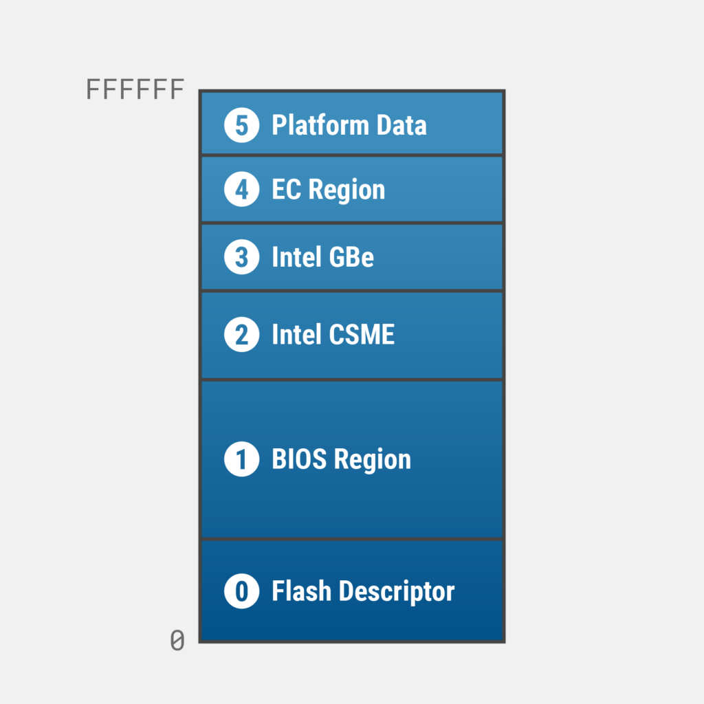
The SPI flash chip is broken out into regions. The first region, region 0, contains the flash descriptor. Think of the flash descriptor as the map to the remaining regions as it contains the locations and access permissions to the SPI flash (among other things as it has an entire layout of its own). While the region locations may vary, with the exception of the flash descriptor being the first region, in the above example region 1 contains the BIOS (UEFI) and region 2 is Intel ME (See Part 2 for more information on Intel ME). The inclusion of remaining regions may vary and can contain firmware for gigabit ethernet adapters, embedded controllers, and additional platform data (These are not well documented publicly and perhaps an area of potential new research). You can use Chipsec to view the SPI flash regions on your system using the following command:
$ sudo ./chipsec_util.py spi info

------------------------------------------------------------
Flash Region             | FREGx Reg | Base     | Limit
------------------------------------------------------------
0 Flash Descriptor       | 00000000  | 00000000 | 00000FFF
1 BIOS                   | 1FFF1000  | 01000000 | 01FFFFFF
2 Intel ME               | 08410081  | 00081000 | 00841FFF
3 GBe                    | 00007FFF  | 07FFF000 | 00000FFF
4 Platform Data          | 00007FFF  | 07FFF000 | 00000FFF
5 Flash Region 5         | 00007FFF  | 07FFF000 | 00000FFF
If the appropriate settings are in place (and these settings will vary across chipsets), in order to write to the SPI flash the processor must be put in SMM (System Management Mode). SMM is the most privileged operating mode (for x86 processors) and may only be invoked with an SMI (System Management Interrupt) and as the name suggests halts all other operations. SMI handlers are accessed via SMRAM (System Management RAM), a special region of RAM reserved for the SMI handling code to live. The SMI handlers communicate with the SPI controller on the chipset (an ICH, I/O Controller hub, or a PCH, Platform Controller Hub), which communicates with the SPI flash storage itself. It’s a bit daunting to consume in just one paragraph, but below is a diagram for some visual representation:
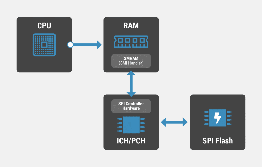
The SPI controller contains registers that are both manufacturer (Intel, AMD) and generation specific (e.g SandyBridge vs Coffee Lake). The register address ranges indicate read and write operations. They are set in the SPI controller, which in turn, communicates directly with the SPI flash.
SPI Flash Write Protections
Now that we’ve walked through some of the fundamentals of how the firmware and configuration are accessed on the SPI flash chip, let’s run through the protections. In general, there are four mechanisms that work together to protect the SPI flash from unauthorized writes:
#1 The Flash Descriptor
Registers in the SPI flash descriptor region (specifically the Master) decide which regions are protected, including the flash descriptor region itself. If the flash descriptor region itself is not protected this means an attacker can change the permissions to give themselves more access (and yes, this sometimes happens, examples to follow). I liken this to setting up a firewall and giving the Internet access to change all of your firewall rules.
You can check for this using Chipsec (we covered how to install Chipsec in Part 2 of this series). First, issue the command to dump the contents of the SPI flash:
$  sudo ./chipsec_util.py spi dump fd.bin


[CHIPSEC] Executing command 'spi' with args ['dump', 'fd.bin']

[CHIPSEC] Dumping entire SPI flash memory to 'fd.bin'
[CHIPSEC] it may take a few minutes (use DEBUG or VERBOSE logger options to see progress)
[CHIPSEC] BIOS region: base = 0x00300000, limit = 0x00FFFFFF
[CHIPSEC] Dumping 0x01000000 bytes (to the end of BIOS region)
[spi] reading 0x1000000 bytes from SPI at FLA = 0x0 (in 262144 0x40-byte chunks + 0x0-byte remainder)
[CHIPSEC] Completed SPI flash dump to 'fd.bin'
[CHIPSEC] (spi) time elapsed 34.729
Next, issue the command to check the Flash Descriptor region:
$ sudo ./chipsec_util.py spidesc fd.bin


Flash Regions
--------------------------------------------------------
 Region                | FLREGx    | Base     | Limit
--------------------------------------------------------
0 Flash Descriptor     | 00000000  | 00000000 | 00000000
1 BIOS                 | 07FF0300  | 00300000 | 007FF000
2 Intel ME             | 02FF0001  | 00001000 | 002FF000

+ 0x0060 Master Section:
========================================================
+ 0x0060 FLMSTR1   : 0xFFFF0000
+ 0x0064 FLMSTR2   : 0xFFFF0000

Master Read/Write Access to Flash Regions
--------------------------------------------------------
 Region                 | CPU      | ME
--------------------------------------------------------
 0 Flash Descriptor     | RW       | RW
 1 BIOS                 | RW       | RW
 2 Intel ME             | RW       | RW
In the above example, we can see the table listing the first three regions on the SPI flash, and the access rights granted to the CPU and to Intel ME. In both cases, read and write operations are permitted, which means this system is not configured securely.
There is another way to check the flash descriptor region access controls in Chipsec using the “spi_access” module. The “spi_access” module not only enumerates all of the flash regions but checks the access levels and provides you with results indicating permission issues:
$ sudo ./chipsec_main.py -m common.spi_access

[*] Running module: chipsec.modules.common.spi_access
[x][ =======================================================================
[x][ Module: SPI Flash Region Access Control
[x][ =======================================================================
SPI Flash Region Access Permissions
------------------------------------------------------------

BIOS Region Write Access Grant (00):
  FREG0_FLASHD: 0
  FREG1_BIOS  : 0
  FREG2_ME    : 0
  FREG3_GBE   : 0
  FREG4_PD    : 0
  FREG5       : 0
BIOS Region Read Access Grant (00):
  FREG0_FLASHD: 0
  FREG1_BIOS  : 0
  FREG2_ME    : 0
  FREG3_GBE   : 0
  FREG4_PD    : 0
  FREG5       : 0
BIOS Region Write Access (4A):
  FREG0_FLASHD: 0
  FREG1_BIOS  : 1
  FREG2_ME    : 0
  FREG3_GBE   : 1
  FREG4_PD    : 0
  FREG5       : 0
BIOS Region Read Access (CF):
  FREG0_FLASHD: 1
  FREG1_BIOS  : 1
  FREG2_ME    : 1
  FREG3_GBE   : 1
  FREG4_PD    : 0
  FREG5       : 0
[!] WARNING: Software has write access to GBe region in SPI flash
[!] WARNING: Certain SPI flash regions are writeable by software
In my limited testing I did find it fairly common for manufacturers, even on newer 12th Gen Intel platforms, to not protect the Intel GBe region. Perhaps this is an area for further research, however, Eclypsium researchers Mickey Shkatov and Jesse Michael demonstrated using the GBe region to hide code or data in their DEF CON Safe Mode presentation titled Bytes In Disguise. You may also notice in the section titled “BIOS Region Write Access” that in addition to the Intel GBe region being writable (FREG_GBE is set to 1), the BIOS region (FREG_BIOS) is also set to 1. Make sure you review the entire table as on this particular system there are areas within the BIOS region that are set writable in order to allow certain updates or configuration changes. In general, the BIOS region is usually set as writable by the CPU within the Flash Descriptor in order to allow software running on the processor to update the flash when necessary. Other protections discussed in this article are used to protect the BIOS region from unauthorized changes. In the Eclypsium product, if one of your systems has a poorly secured flash descriptor the following finding will be present:
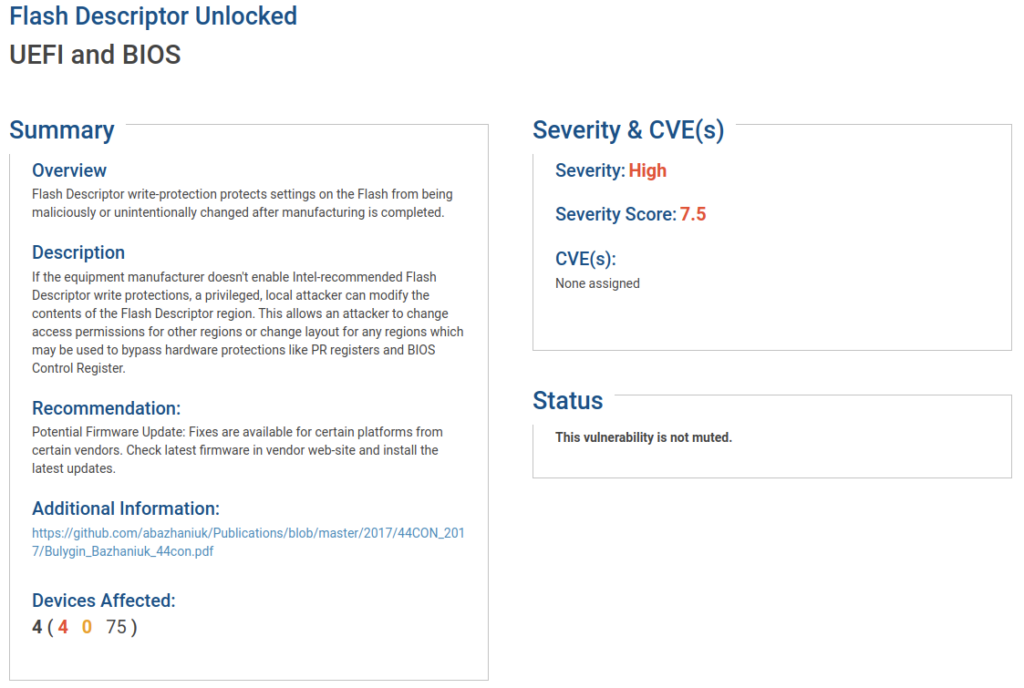
The system scanned above does not have the proper permissions set in the flash descriptor. As indicated above, the flash descriptor itself is writable, meaning an attacker could abuse this misconfiguration to corrupt the flash descriptor region or change the permissions to allow writes.
#2 Global Write Protections
Provided by the chipset (ICH or PCH) these settings control access to the BIOS Region on the SPI Flash. The options are set in the BIOS Control Register and are as follows:
- BIOSWE (BIOS Write Enable) – A value of 0 indicates that only read operations are permitted. A value of 1 indicates the SMI code will be allowed to update the BIOS (provided BLE is set to 1). The important note for this setting is that when this register is written, the value will change first (e.g. from 0 to 1), then the BLE register will be checked and trigger the corresponding SMI!
- BLE (BIOS Lock Enable) – A value of 0 indicates that setting BIOSWE will not result in an SMI if the BIOSWE bit is set. A value of 1 indicates SMIs will be generated if BIOSWE is set to 1. The code running in the SMI handler will then check if this was triggered by an authorized request and set the BIOSWE value back to 0 if it was written by an unauthorized entity. The important note for this setting is that only a platform reset (e.g. system reboot, resume from sleep, power cycle, etc..) will clear the value.
- SMM_BWP (SMM BIOS Write Protect Disable) – This feature was introduced to address issues with BIOSWE and BLE (described below). A value of 0 indicates the BIOS is writable even if processors are not in SMM mode. A value of 1 indicates the BIOS is not writable unless all processors are in SMM mode. This will write-protect the entire BIOS region from software other than an SMI handler executing in SMM mode. In later models of Intel chipsets this is now referred to as “Enable InSMM.STS” (e.g. Intel® 300 Series Chipset Families).
The above settings may be configured in such a way that your system is vulnerable. A race condition exists in the BIOSWE and BLE implementation that presents an opportunity for an attacker to gain write access to your BIOS. This vulnerability and attack are described in a previous blog post titled Protecting System Firmware Storage and the research paper titled Speed Racer: Exploiting an Intel Flash Protection Race Condition. Essentially, BIOSWE is set before the state of BLE is checked, allowing an attacker to continually set BIOSWE via one processor (or thread) while using another process (or thread) to write to the BIOS.
Using the common.bios_wp module in chipsec we can check these settings:
$ sudo ./chipsec_main.py -m common.bios_wp

[x][ =======================================================================
[x][ Module: BIOS Region Write Protection
[x][ =======================================================================
[*] BC = 0x00000888 << BIOS Control (b:d.f 00:31.5 + 0xDC)
    [00] BIOSWE           = 0 << BIOS Write Enable
    [01] BLE              = 0 << BIOS Lock Enable
    [02] SRC              = 2 << SPI Read Configuration
    [04] TSS              = 0 << Top Swap Status
    [05] SMM_BWP          = 0 << SMM BIOS Write Protection
    [06] BBS              = 0 << Boot BIOS Strap
    [07] BILD             = 1 << BIOS Interface Lock Down
[-] BIOS region write protection is disabled!
The above configuration leaves the system vulnerable to the attacks mentioned above as BIOSWE, BLE and SMM_BWP are all set to 0.
#3 BIOS Range Write Protection
Protected range (PR) registers allow you (typically the hardware manufacturer) to define address ranges in the SPI flash that are protected, even from SMI handers. These registers and values are writable only when the flash is unlocked (See below for a description of flash locking, yet another protection mechanism for the SPI flash). The values are based on FLAs (Flash Linear Addresses, the addresses that correspond to locations on the SPI flash chip).
Using the same common.bios_wp chipsec module we can check these settings as well:
$ sudo ./chipsec_main.py -m common.bios_wp

[*] BIOS Region: Base = 0x00300000, Limit = 0x00FFFFFF
SPI Protected Ranges
------------------------------------------------------------
PRx (offset) | Value    | Base     | Limit    | WP? | RP?
------------------------------------------------------------
PR0 (84)     | 00000000 | 00000000 | 00000000 | 0   | 0
PR1 (88)     | 00000000 | 00000000 | 00000000 | 0   | 0
PR2 (8C)     | 00000000 | 00000000 | 00000000 | 0   | 0
PR3 (90)     | 00000000 | 00000000 | 00000000 | 0   | 0
PR4 (94)     | 00000000 | 00000000 | 00000000 | 0   | 0

[!] None of the SPI protected ranges write-protect BIOS region

[!] BIOS should enable all available SMM based write protection mechanisms.
[!] Or configure SPI protected ranges to protect the entire BIOS region.
[-] FAILED: BIOS is NOT protected completely
Both Global write protections (#2) and BIOS range write protections (#3) are covered in Eclypsium’s product under “Missing BIOS Write Protections” and carry a severity score of 8.2:

#4 Flash Configuration Lockdown
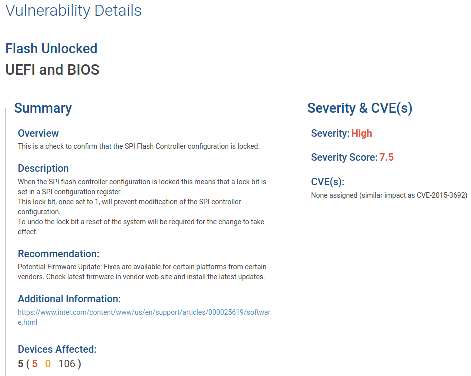
We’ve discussed how to modify write permissions in a few different ways and you may be wondering how to prevent malicious actors from modifying these settings (essentially undoing the protections). Intel provides the FLOCKDN lock bit (Flash Lockdown) within the SPI controller to solve this problem. This is a hardware mechanism implemented in the chipset, such that when a value of 1 is written to FLOCKDN, it will lock itself and select other settings based on the chipset generation. Specifically for PRs (and perhaps other chipset configurations depending on which one is included with your computer), locking them is important. The FLOCKDN bit, once locked, can only be unlocked upon a platform reset. On several of my systems, thankfully, this bit has been set. I confirmed this using Chipsec:
$ sudo ./chipsec_main.py -m common.spi_lock

[*] Running module: chipsec.modules.common.spi_lock
[x][ =======================================================================
[x][ Module: SPI Flash Controller Configuration Locks
[x][ =======================================================================
[*] HSFS = 0x3F00E800 << Hardware Sequencing Flash Status Register (SPIBAR + 0x4)
    [00] FDONE            = 0 << Flash Cycle Done
    [01] FCERR            = 0 << Flash Cycle Error
    [02] AEL              = 0 << Access Error Log
    [05] SCIP             = 0 << SPI cycle in progress
    [11] WRSDIS           = 1 << Write status disable
    [12] PR34LKD          = 0 << PRR3 PRR4 Lock-Down
    [13] FDOPSS           = 1 << Flash Descriptor Override Pin-Strap Status
    [14] FDV              = 1 << Flash Descriptor Valid
    [15] FLOCKDN          = 1 << Flash Configuration Lock-Down
    [16] FGO              = 0 << Flash cycle go
    [17] FCYCLE           = 0 << Flash Cycle Type
    [21] WET              = 0 << Write Enable Type
    [24] FDBC             = 3F << Flash Data Byte Count
    [31] FSMIE            = 0 << Flash SPI SMI# Enable
[+] SPI write status disable set.
[+] SPI Flash Controller configuration is locked
[+] PASSED: SPI Flash Controller locked correctly.
In the Eclypsium product we also have a test for this condition and I was able to find an example of a vulnerable system:
Conclusion
As we’ve outlined in this article there are several mechanisms available to restrict write access to the SPI flash where critical system firmware and configuration are stored. The available mechanisms also have interdependencies. For example, the manufacturer may have set BLE (BIOS Lock Enabled), but not set SMM_WP, leaving your system vulnerable to the Speed Racer attack. Given that firmware and settings can be changed and updated, this does not always indicate the updates will be more secure. I’ve experienced firmware updates that may fix a bug (or several), but undo some important security configuration. Attackers are looking for easy ways to hide in UEFI to maintain persistence and will look for these flaws in your systems (e.g. Trickboot). It is important to continually monitor BIOS configuration to ensure the appropriate configuration is in place and implement a system that alerts you if something has changed.
Special thanks to those at Eclypsium who collaborated with me to write this article: Jesse Michael, Mickey Shkatov, John Loucaides, and Alex Bazhaniuk.
References
- Trickbot Now Offers ‘Trickboot’: Persist, Brick, Profit
- Checking BIOS protections offline with just the firmware updates – Yuriy Bulygin at 44CON 2017 (Video)
- Speed Racer: Exploiting an Intel Flash Protection Race Condition
- Advanced x86: Introduction to BIOS & SMM – A free course from John Butterworth and Xeno Kovah. Also, be certain to check out Xeno’s newer free training offerings at Open Security Training 2.
- Intel® 7 Series / C216 Chipset Family Platform Controller Hub (PCH) Datasheet
Resources
- Using Intel TXT to Attack BIOSes
- CVE-2017-8083: Intense PC lacks BIOS Write Protection
- Evil Maid Just Got Angrier Why Full-Disk Encryption With TPM is Insecure on Many Systems
- https://twitter.com/c7zero/status/846541211431141376 – Missing BIOS Write Protections example and discussion
- Gigabyte BRIX BIOS Write Protection is not enabled
- Hardening tweaks via CHIPSEC framework
- https://nvd.nist.gov/vuln/detail/CVE-2018-4251 – SPI flash writes + ME manufacturing mode
- Intel BIOS locking mechanism contains race condition that enables write protection bypass